
Полная версия
All sciences. №1, 2023. International Scientific Journal
Next, the signal from the output of the threshold device 14 (Fig.2.2.d) is fed to one of the inputs of the matching circuit 15. A signal is sent to the other input of the matching circuit 15 from the output of the second differentiating device 16 (Fig.2.e).
From the moment of comparing tc, a series of pulses appears at the output of the coincidence circuit 15, which arrive at the counting input of the counter 17 (Fig.2.2.g).
At the beginning of the next exponent, rectangular pulses from the output of one vibrator 4 arrive at the input "Zero setting" of the counter 17 and the counter 17 is prepared. According to the meter readings, the concentration of CO2 gases can be determined.
The optoelectronic device uses LEDs based on GaAlAsSb/GaInAsSb/GaAlAsSb (3.12 microns) as the emitting diode at the reference wavelength, and LEDs based on GaAlAsSb/GaInAsSb/GaAlAsSb (3.39 microns) as the emitting diode at the measuring wavelength.
A PD36 series photodiode for the spectral range of 1.5—3.8 microns based on the InAs/InAsSbP heterostructure was used in an optoelectronic device for monitoring the CO2 content in the atmosphere.
Literature
1. Avezov R. R., Lutpullaev S. L. The state, prospects and problems of using renewable energy sources in Uzbekistan. // Conference dedicated to the Year of Physics – 2005 Tashkent, September 27 – 28, 2005, p.119.
2.Berman E. Geothermal Energy. Translated from English edited by Dr. B.F. Mavritsky. Mir Publishing House, Moscow. 1978. – 167s.
3. Alkhasov A. B. Geothermal energy: problems, resources, technologies. M.: Fizmatlit, 2008. 376 p.
4. Processes of heat and mass transfer in the complex use of geothermal resourses: Monograph / V. V. Potapov, M. A. Bliznyukov, S. A. Smyvalov, V. A. Gorbach. – Petropavlovsk-Kamchatsky: Kamchatstu, 2005. – 136 p.
HUMIDITY METER ON SEMICONDUCTOR EMITTERS
UDC 621.38
Qo’ldashov Obbozjon Xokimovich
Doctor of Technical Sciences, Professor of the Scientific Research Institute «Physics of Semiconductors and Microelectronics» at the National University of Uzbekistan
Sayfullaev Xamidullo Turg'unbay ugli, Boltaboev Javohir Jakhongir o'g'li
2nd year masters of the Department of «Physics of Semiconductors and Polymers» of the Faculty of Physics of the Mirzo Ulugbek National University of Uzbekistan
Scientific Research Institute "Physics of Semiconductors and Microelectronics" at the National University of Uzbekistan
Annotation. The article proposes a humidity meter based on semiconductor emitters. The spectral characteristics of humidity and LED are given. A block diagram of a humidity meter on semiconductor emitters is given.
In the humidity meter on semiconductor emitters, LEDs based on GaAlAsSb/GaInAsSb/GaAlAsSb (2.2 microns) are used as a emitting diode at the reference wavelength, and LEDs based on GaAlAsSb/GaInAsSb/GaAlAsSb (1.94 microns) are used as a emitting diode at the measuring wavelength.
Keywords: optoelectronics, spectra, absorption, LEDs, photodiodes, device, mathematical model, block diagram, microprocessor unit.
Аннотация. В статье предложен измеритель влажности на полупроводниковых излучателях. Приведены спектральные характеристики влажности и светодиода. Приведена блок схема измерителя влажности на полупроводниковых излучателях.
В измерителе влажности на полупроводниковых излучателях использованы в качестве излучающего диода на опорной длине волне светодиоды на основе GaAlAsSb/GaInAsSb/GaAlAsSb (2.2 мкм), а излучающего диода на измерительной длине волны светодиоды на основе GaAlAsSb/GaInAsSb/GaAlAsSb (1.94 мкм).
Ключевые слова: оптоэлектроника, спектры, поглощение, светодиоды, фотодиоды, устройство, математическая модель, блок схема, микропроцессорный блок.
Introduction
The basis of optoelectronic methods and devices are emitters and photodetectors. The widespread use of optoelectronic methods was hindered by the lack of simple reliable radiation sources. The appearance of semiconductor radiation sources has significantly expanded the scope of application of optoelectronic methods and devices [1].
At present, semiconductor emitters with a radiation spectrum ranging from the ultraviolet section to the near infrared section of the optical spectrum have been developed and are being mass-produced. Practically at present, it is possible to develop emitters in the range from 210 to 4000 microns with spectral characteristics close to monochromatic (with quasi-monochromatic spectral characteristics). The features of semiconductor emitters are high speed, the ability to control the radiation flow by current, monochromaticity, sufficient radiation power and small overall dimensions. The presence of such advantages in semiconductor emitters creates prerequisites for the research and development of various monitoring, measurement and conversion devices for various fields of science and technology. Hence follows a wide range of work in the field of creating devices and systems based on semiconductor emitters [2].
The basis of optical methods and devices is the presence of an emitter and an optically connected photodetector through the medium. The radiation generated by the emitter, passing through the medium (air, substance, etc.), is perceived by the photodetector. In these methods and devices, optical radiation is used as a data carrier that does not create electromagnetic interference and is not affected by these interference. The presence of such a feature and the simplicity of the instrument implementation create prerequisites for the research and development of various devices based on the use of optical radiation [3].
The main part
To build a moisture meter on semiconductor emitters, the property of water to absorb IR radiation of a certain wavelength is important [4]. All substances and materials have a certain hygroscopicity and, therefore, absorb moisture from the external environment. The analysis of spectral characteristics showed that the absorption bands lie in the range of 0.76…0.97 and 1.19…1.94 microns [5].
Table 1 shows the absorption spectra of water and their affiliation.
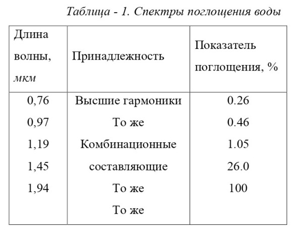
From the different spectral characteristics of dry matter (Fig. 1, curve 1) and at a humidity of 9% H2O (curve 2), it follows that at a wavelength of 1.94 microns, water has significant absorption [6]. In the humidity meter on semiconductor emitters, LEDs with radiation spectra of 2.2 microns are used as a reference channel, and LEDs with radiation spectra of 1.94 microns are used as a measuring channel).
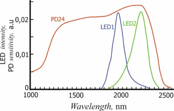
Fig. 1. Emission spectra of LED1, LED2 LEDs and spectral sensitivity of PD24 photodiode.
LEDs based on the semiconductor compound GaSb and its solid solutions GaInAsSb and AlGaAsSb have been developed to measure the moisture content of raw cotton. LED structures are manufactured by the FEF method and grown on Gaas n-type conductivity substrates doped with Te to an electron concentration of 8·1017 cm-3. The emitters for measuring the moisture content of raw cotton consisted of an active layer of n – GaInAsSb (Eg = 0.51 eV) 2—3 microns thick and grown on n – GaSb substrates and doped with Te to a charge carrier concentration of 9·1017 cm—3, the wide-band emitter p – AlGaAsSb, doped with germanium to a concentration of 5·1018 cm-3 (fig.2).
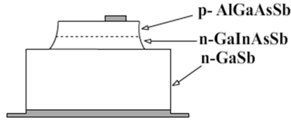
Fig.2. GaSb-based LED for humidity measurement.
LEDs based on the GaSb semiconductor compound for measuring the humidity of raw cotton at a temperature of 24 0C had an external quantum photon output of 5.9 – 6.5% and an optical power of 3.9 MW in direct current.
To maximize the output of optical radiation, the TO-18 housing with a parabolic reflector is used, which allows collimating radiation at an angle of 10—11o. Figure 3 shows the design of the IR LED:
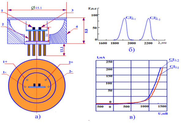
Fig. 3. LED with a parabolic reflector: a) design, b) radiation spectra, c) VAC (where: 1 – LED chip (1.94 microns), 2 – thermal cooler, 3 – LED chip (2.2 microns), 4 – parabolic reflector)
LEDs based on the GaAlAsSb/GaInAsSb/ GaAlAsSb double heterostructure had a quantum yield of 5.8%, a radiation wavelength of 1.94 microns for measuring the moisture content of raw cotton, its main parameters are shown in Table 2.
The proposed design provides equal conditions for two LED crystals, thus eliminating the time and temperature instabilities of their main parameters.
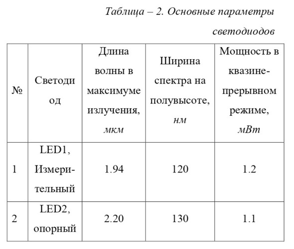
Fig. 3 shows a block diagram of a digital humidity meter, which consists of the following elements: a master generator – ZG; trigger – T; frequency divider – DC; differentiating devices – DU1, DU2; exponent modulator – ME; emitter repeater – EP; pulse amplifier – IU; radiation receiver – AF; low – noise amplifier – MSU; matching circuit – SS; counter – SCH; decoder – DS; indicator – IN; reference LED – ID1; measuring LED – ID2.

Fig.4. Block diagram of a humidity meter on semiconductor emitters
The characteristic features of the humidity meter on semiconductor emitters are high selectivity, sensitivity, accuracy and reproducibility of measurements, as well as the possibility of continuous non-destructive testing, contactless and rapid analysis.
Conclusion
To create a humidity meter on semiconductor emitters, the optimal absorption band free from the absorption band of interfering components l1 = 1.94 microns has been determined.
The optoelectronic device uses LEDs based on GaAlAsSb/GaInAsSb/GaAlAsSb (2.2 microns) as the emitting diode at the reference wavelength, and LEDs based on GaAlAsSb/GaInAsSb/GaAlAsSb (1.94 microns) as the emitting diode at the measuring wavelength.
The absolute error of the moisture content measurement results was 0.5%.
Literature
1. Bashkatov A. S., Mescherova D. N. «The main trends in the development of optoelectronic technology until 2030,» Abstracts of the Russian Conference and School of Young scientists on current problems of semiconductor photoelectronics «Photonics-2019», 2019, doi: 10.34077/rcsp2019—25. pp.25—26.
2. Bogdanovich M. V. «Water content meter in oil and petroleum products based on infrared optoelectronic LED-photodiode pairs,» Journal of Technical Physics, 2017, doi:10.21883/jtf.2017.02.44146.1791.
3. Masharipov Sh. M. Analysis of modern methods and technical means of measuring humidity of cotton materials. // Devices, 2016, No. 4., pp. 31—37.
4. Demyanchenko M. A. Absorption of infrared radiation in a multilayer bolometric structure with a thin metal absorber // Optical Journal. – 2017. Volume 84 – pp. 48—56.
5. Rakovics V., Imenkov A. N., Sherstnev V. V., Serebrennikova O. Yu., Ilyinskaya N. D., Yakovlev Yu. P. «Powerful LEDs based on InGaAsP/InP heterostructures,» fiz. i tekhnika poluprovodn., 2014.t.48.s.1693—1697.
6. Artemov V. G., Volkov A. A., Sysoev N. N. «The absorption spectrum of water as a reflection of charge diffusion // Izvestia of the Russian Academy of Sciences. Physical series, Proceedings of the Russian Academy of Sciences. The series is physical. – 2018. – vol.82. – pp. 67—71. doi: 10.7868/s0367676518010143.
DEVICES FOR REMOTE TEMPERATURE CONTROL BASED ON LEDS (λ=2.0 microns)
UDC 621.38
Qo’ldashov Obbozjon Xakimovich
Doctor of Technical Sciences, Professor of the Scientific Research Institute "Physics of Semiconductors and Microelectronics" at the National University of Uzbekistan
Ergashev Doniyor Jamoliddin ugli
2nd year Master of the Department of "Physics of Semiconductors and Polymers" of the Faculty of Physics of the Mirzo Ulugbek National University of Uzbekistan
Scientific Research Institute "Physics of Semiconductors and Microelectronics" at the National University of Uzbekistan
Annotation. An optoelectronic device for remote temperature control of small-sized objects is proposed, which can be successfully used in the study of temperature characteristics of solar installations.
Keywords: temperature, optoelectronics, sensor, control, LED, photodiode, block diagram, design.
Аннотация. Предложено оптоэлектронное устройство для дистанционного контроля температуры малоразмерных объектов, которое может быть успешно использовано при исследовании температурных характеристик гелиотехнических установок.
Ключевые слова: температура, оптоэлектроника, датчик, контроль, светодиод, фотодиод, блок схема, конструкция.
The device for remote temperature control contains a monitoring object 1, which through a modulator 2 is optically connected to the first radiation receiver 3, whose output is through the first amplifier 4, the first amplitude detector 5 and the first integrator 6, connected to the first input of the signal ratio receiving device 13, the second radiation receiver 7, whose output is through the second amplifier 8, the second amplitude detector 9 and the second integrator 10 are connected to the second input of the signal ratio receiving device 13 whose output is connected to the input of the recording device 14, the control device of the source of the collimated radiation 12, the input of which is connected to the output of the first amplifier 4, and the output is connected to the input of the source of the collimated radiation 11, which, through reflection from the surface of the controlled object 1, is optically connected to the second radiation receiver 7, an electric motor 15, the rotor of which is mechanically connected to the axis of rotation of the modulator 2. In Fig.4.13. the design of the modulator is shown. Here: 16 is the axis of rotation of the modulator; 17 is the modulating holes; 18 is a metal disk. Figure 4.14 shows time diagrams explaining the principle of operation of the proposed device. Figure 1 shows a block diagram, and Figure 2 shows the sensor design.
The optoelectronic device works as follows. The thermal radiation flux FPI1 (λ) of the control object 1, which is proportional to its temperature, passes the distance l, is modulated by the modulator 2 and enters the sensitive area of the first radiation receiver. The flux reaching the sensitive area of the first radiation receiver, according to the theory of optoelectronic devices, is defined as:
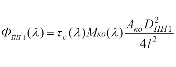
where: tc (λ) is the spectral transmittance of the atmosphere; Mco (λ) is the spectral density of the energy luminosity radiating from the surface of the controlled object; Ako is the area of the radiating surface of the controlled object; DP1 is the diameter of the entrance pupil of the first radiation receiver; l is the distance between the controlled object and the first photodetector.
Table 1 shows the main characteristics of photodiodes
Considering that

expressions (1) will take the form:
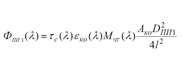
where: eko (λ) is the spectral coefficient of thermal radiation of the controlled object; MCHT (λ) is the spectral density of the energy luminosity of the black body. Considering that the radiation receiver operates in a limited spectral range, expression (2) for wavelengths λ1m, which corresponds to the maximum sensitivity of the first radiation receiver, can be written as:
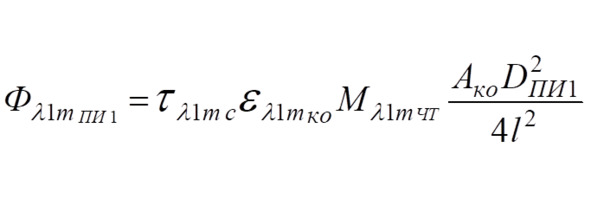
where: ελ1mk0 is the spectral coefficient of thermal radiation of the controlled object at wavelengths λ1m; Mλ1mcht is the spectral density of the energy luminosity of the black body at wavelengths λ1m; τλ1mc is the transmittance of the atmosphere at wavelengths λ1m.
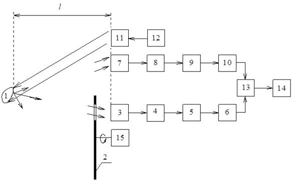
Fig.1. Block diagram of an optoelectronic device.
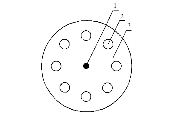
Fig.2. The design of the modulator.
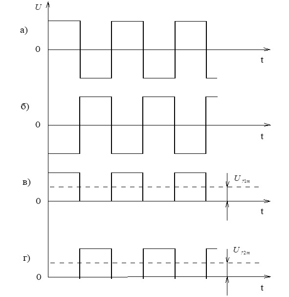
Fig.3. Time diagrams of an optoelectronic device.
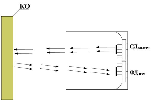
Fig.4. Sensor design.
Taking into account the Stefan-Boltzmann law that Mλ1mcht=σT4, expression (4) will take the form:
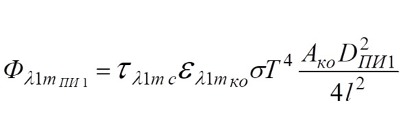
where: T is the temperature of the controlled object; σ=5.6697*10-8 W*m-2*K-4 is the Stefan-Boltzmann constant.
In addition, the sensitive area of the first radiation receiver 3 is affected by the heat flux of radiation from the modulator 2, which can be described by the ratio
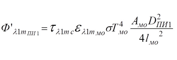
where: ελ1mm0 is the spectral coefficient of thermal radiation of the modulator at wavelengths λ1m; Tmo is the temperature of the modulator; Amo is the area of the radiated surface of the modulator; lmo is the distance between the modulator and the first radiation receiver.
Therefore, the total flux acting on the sensitive area of the first radiation receiver has the form.
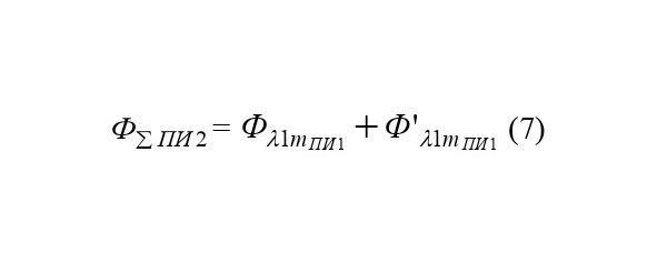
Then the output voltage of the first radiation receiver is defined as:
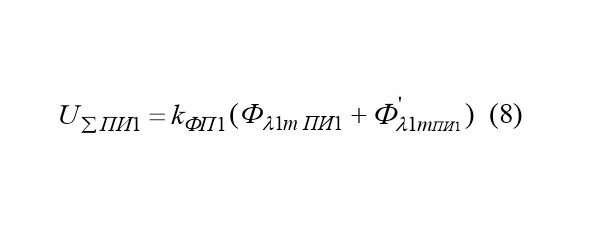
or
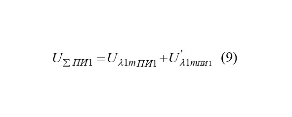
where: is the transmission coefficient of the first radiation receiver.
The voltage corresponding to expression (9) from the output of the second radiation receiver 3 is amplified by the first amplifier 4, as a result of which an alternating electrical signal is formed at its output (see Fig. 3.c) the amplitude of which is defined as:
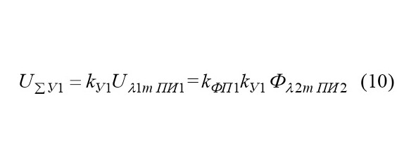
where ky1 is the transmission coefficient of the first amplifier 4.
Since due to the use of a disk modulator with symmetrical modulating holes, the thermal radiation of the modulator itself, which affects the sensitive area of the first radiation receiver during the modulation period remains constant (see Figure 3a), i.e.

Therefore, the constant component of the total signal of the first radiation receiver 3 does not pass through the AC amplifier 4. That is, the amplitude of the variable component of the amplified signal is proportional only to the amplitude of the flux Fλ1mPI1.
The variable component of the amplified signal is detected by the first amplitude detector 5. The detected signal (see Figure 3.d) from the output of the first amplitude detector 5 is integrated by the first integrator 6 and fed to the first input of the signal ratio device 13.
In this case, the voltage supplied to the first input of the signal ratio receiving device 13, taking into account the above, can be described by the expression:
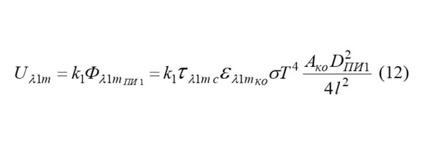
where k1=kPI1kU1kAD1kINT1 is the total transmission coefficient of blocks connected in series with the first radiation receiver 3, the first amplifier 4, the first amplitude detector 5 and the first integrator 6; kAD1 is the transmission coefficient of the first amplitude detector; kINT1 is the transmission coefficient of the first integrator.
When the output signal of the first amplifier 4 is exposed to the input of the control device of the collimated radiation source 12, an antiphase electrical signal is formed at its output. The latter is fed to the input of the collimated radiation source 11 and causes a pulsed flow of collimated radiation at its output.
The formed flow, by the source of collimated radiation 11, is induced to the area of the controlled object 1. In this case, the flow reaching the surface of the controlled object 1 in the case Ako ≤ Aki is defined as:
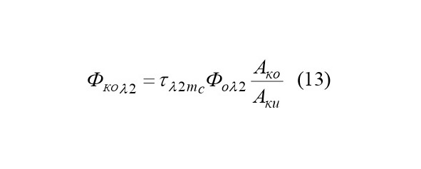
where Aki is the cross – sectional area of collimated radiation; τλ2mc is the transmittance of the atmosphere at wavelengths λ2m; Foλ2 is the initial flux of collimated radiation. In this case, the reflected flow from the surface of the controlled object 1 is defined as:
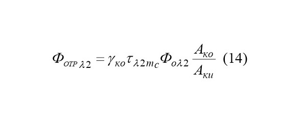
where uco is the reflection coefficient of the surface of the controlled object at wavelengths λ2.
In this case, the expression for the reflected modulated flux from the surface of the controlled object and reaching the sensitive area of the second radiation receiver 7 has the form:
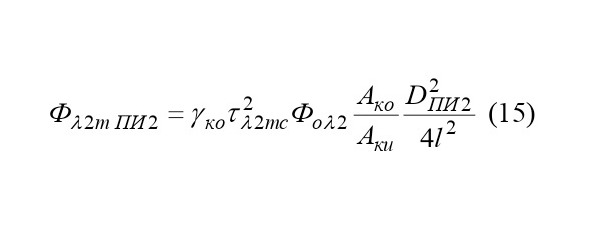
where: DPI2 is the diameter of the entrance pupil of the second radiation receiver.
In addition, in the case of a partial coincidence of the radiation spectrum of the controlled object with the spectral sensitivity of the second radiation receiver 7, an unmodulated radiation flux from the controlled object at a wavelength of λ2m affects the sensitive area of the latter.
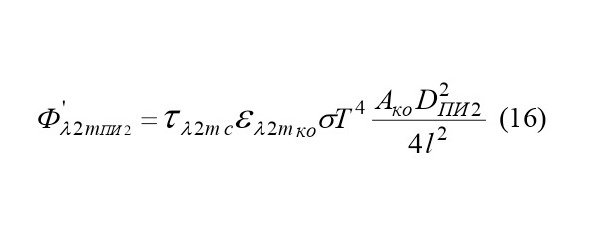
where: ελ2m is the spectral coefficient of thermal radiation of the controlled object at wavelengths λ2m;
Then the total radiation flux acting on the sensitive area of the second radiation receiver 7 has the form.
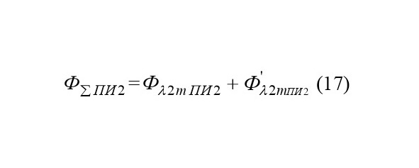
Therefore, the output voltage of the second radiation receiver is defined as:
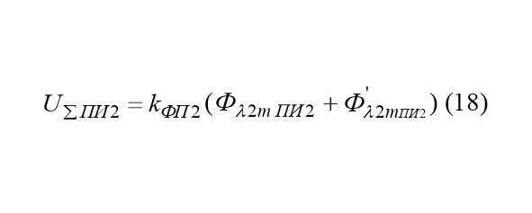
or
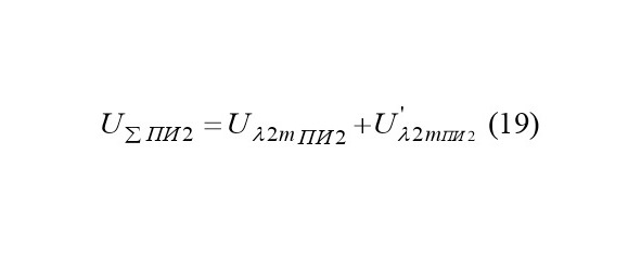
where cFP2 is the transmission coefficient of the second radiation receiver.
The voltage corresponding to expression (18) from the output of the second radiation receiver 7 is amplified by the second amplifier 8, as a result of which an alternating electrical signal is formed at its output (see Fig.3. d) the amplitude of which is defined as:
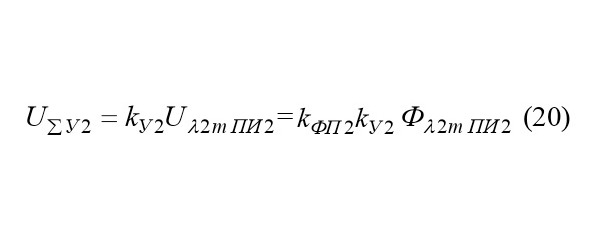
where ky2 is the transmission coefficient of the second amplifier 8.
Since during the period the repetition of the modulation Uλ2mPI2 can be considered constant, i.e. (see Fig. 3.b)

Therefore, the constant component of the total signal of the second radiation receiver 7 does not pass through the AC amplifier 8. That is, the amplitude of the alternating component of the amplified signal is proportional only to the amplitude of the flux Fλ2mPI2.


